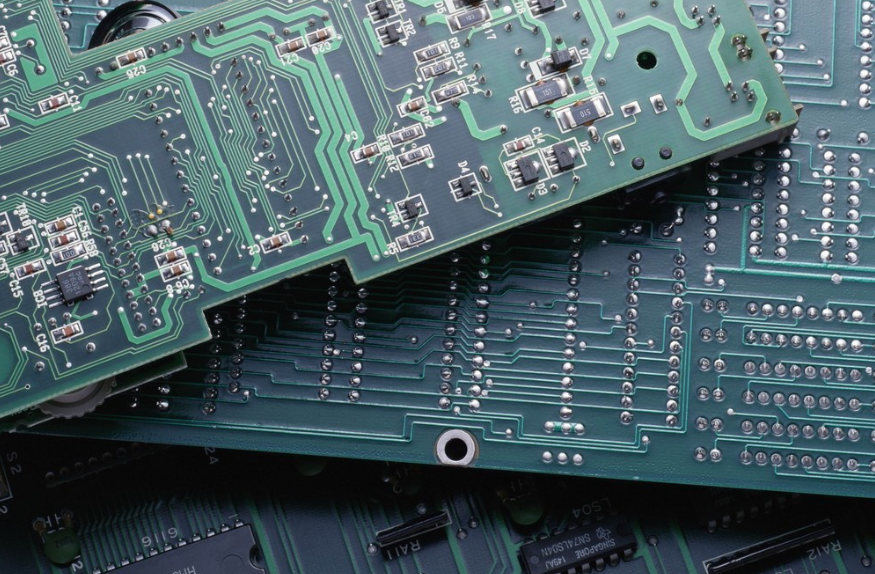
What is High density interconnect PCB?
High-density interconnect PCB achieves higher wiring density by using structures such as blind holes and buried holes. This PCB design enables the integration of more components and connections within a limited space, thus meeting the requirements of modern electronic devices for high performance, lightweight, and high reliability. As electronic products continue to evolve towards miniaturization and multi-functionality, High density interconnect PCB has become a key technology in fields such as smart phones, medical equipment, and automotive electronics, driving innovation and progress in the electronics industry.
The technical features of High Density Interconnect PCB
The high-density interconnect PCB employs multi-layer stacking and micropore technology. The hole diameters are usually less than 150um, and the line width and spacing can be controlled below 50um, thereby significantly increasing the wiring density. This PCB uses blind and buried holes to reduce the inter-layer distance, improve the signal transmission path, and reduce latency and crosstalk. These features enable it to support high-frequency signal transmission and high-speed data processing, and are suitable for high-end applications such as 5G communication, artificial intelligence, and IoT devices. Through optimized layout, the High density interconnect PCB can also reduce electromagnetic interference and improve the overall system reliability.
The main reason for adopting HDI PCB
The main reasons for using HDI PCBs include enhancing performance, reducing product size and lowering costs.
Firstly, the high-density wiring allows for shorter signal paths, thereby reducing transmission delay and power consumption, and improving the response speed of the equipment.
Secondly, this type of PCB supports the miniaturization and integration of components, helping manufacturers design thinner and more portable electronic products, such as wearable devices and drones.
Moreover, HDI PCBs optimize the production process by reducing the number of layers and material usage, thereby lowering the overall manufacturing cost and failure rate.
From a market perspective, adopting this technology can accelerate product launch time, enhance competitiveness, and meet environmental requirements, reducing resource waste. In summary, High density interconnect PCBs are a key factor in promoting the sustainable development of the electronics industry, and will play an important role in more fields in the future.