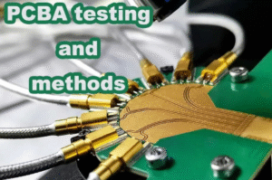
Quality Inspection
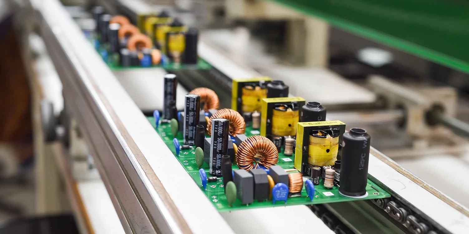
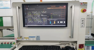
We use advanced MES for production line control ,with Fuji NXT,MPM, JUKI, Desen, Suneast and other industry professional equipment, which covers automatic surface mount system , reflow soldering, automatic testing and packaging processes,and production workshop using a fully enclosed air-conditioning system ,temperature and humidity and lighting intensity control ,high standards of electrostatic protection managerment.


-
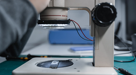
Visual inspection
-
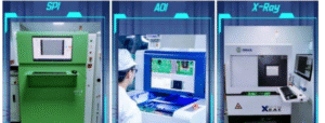
X-ray Inspection
-
3D AOI Testing
-
ICT (In-Circuit Test)
-
FAI
-
AOI Testing
-
3D SPI Testing
-
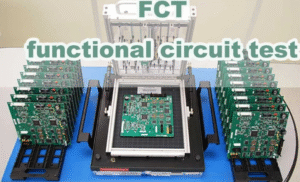
Functional Test
Visual inspection
Manual visual inspection is a method that confirms the component placement on a PCB through human vision and comparison. This technique is one of the most widely used online testing methods. However, as production volume increases and circuit boards and components become smaller, this method becomes increasingly less applicable. Its main advantages are low upfront costs and the absence of test fixtures; at the same time, its main disadvantages include high long-term costs, discontinuous defect detection, difficulty in data collection, lack of electrical testing, and visual limitations.
X-Ray Test
Also known as X-ray inspection, uses low-energy X-rays to quickly detect problems such as open circuits, short circuits, missing solder joints, and incomplete soldering on circuit boards.
X-ray is mainly used to detect defects in circuit boards with extremely small spacing and extremely high density, as well as defects such as bridging, chip missing, and misalignment that occur during assembly. It can also use tomography to detect internal defects in IC chips. This is the only method for testing the quality of ball grid array and solder bump bonding. The main advantage is that it can inspect BGA solder quality and embedded components without the need for fixed devices.
3D AOI Testing
3D AOI stands for 3D automated optical inspection. 3D AOI inspects assembled printed circuit boards and other electronics in three dimensions. This is in contrast to 2D AOI or two-dimensional automated optical inspection. This typically involves a camera to verify that the items meet quality standards, whether making sure it is the right size or items are in their proper locations.
ICT (In-Circuit Test)
ICT, which stands for Automatic Online Testing, is an essential testing equipment for modern PCB manufacturers and is very powerful. It mainly detects the open circuits, short circuits of the PCBBA’s circuits, and the faults of all components by testing the contact points on the PCB layout with the test probes, and clearly informs the staff.
ICT has a wide range of applications, high measurement accuracy, and clearly indicates the detected problems. Even workers with average electronic technical skills can handle faulty PCBA very easily. Using ICT can greatly enhance production efficiency and reduce production costs.
FAI
PCBA FAI (First Article Inspection) is a quality control process in which a manufactured PCBA is inspected to ensure that it meets the design specifications and requirements. It is typically carried out at the beginning of the manufacturing process, before mass production starts.
During the PCBA FAI process, a sample of the PCBA is inspected and measured to verify that they meet the required tolerances, dimensions, and other specifications. The process includes visual inspection, measurement of physical characteristics, and functional testing to ensure that the PCBA are of high quality and fit for their intended use.
The PCBA FAI process is important because it helps to identify and address any issues or defects in the manufacturing process early on, which can save time and resources by preventing the production of defective PCBs. It is typically carried out by a trained and experienced quality control technician or engineer.
AOI Testing
Automated optical inspection (AOI) technology, also known as machine vision inspection (MVI) technology or automated visual inspection (AVI) technology. In some industries, such as flat panel display, semiconductor, solar, and other manufacturing industries, the term AOI is more popular and known. But AOI and MVI / AVI are still slightly different in concept and function.
In a narrow sense, MVI is an emerging scientific technology that integrates image sensing technology, data processing technology, motion control technology, and performs tasks such as measurement, detection, recognition, and guidance in the industrial production process. The basic principle of MVI uses optical imaging methods (such as a camera, or a complex optical imaging system) to simulate the visual imaging function of the human eye, use a computer processing system instead of the human brain to perform data processing, and finally feedback the results to the implementing agency (such as mechanical Hand) to complete various prescribed tasks instead of manpower.
Broadly speaking, MVI is a technology that stimulates and expands the functions of human eyes, brains, and hands. Its definition may have subtle differences in different application areas, but they cannot leave two fundamental methods and technologies. Obtain the required information from the image, and then feed it back to the automatic actuator to complete the specific task. It can be said that the automatic detection technology based on any image sensing method (such as visible light imaging, infrared imaging, X-ray imaging, ultrasound imaging, etc.) can be considered as MVI or AVI. When using optical imaging methods, MVI actually becomes AOI. Therefore, AOI can be regarded as a special case of MVI.
According to different imaging methods, AOI can be divided into three-dimensional (3D) AOI and two-dimensional (2D) AOI. The three-dimensional AOI is mainly used for the measurement of object shape and geometric parameters, part grouping, positioning, recognition, robot guidance, etc.; AOI is mainly used for product appearance (color, defects, etc.) detection, classification of different objects or appearances, detection, and classification of good and defective products, etc.
3D SPI Testing
3D solder paste inspection, also called SPI is a technique for testing printed circuit boards to make sure that they are printed correctly. You use a machine to monitor the solder paste alignment and volume during the printing process.
3D SPI (Solder Paste Inspection) testing is a process used to inspect and verify the quality of the soldering process in the manufacturing of electronic devices. Solder paste is a material used to join electronic components to a printed circuit board (PCB) during the manufacturing process. 3D SPI testing is a non-destructive inspection method that uses a 3D imaging system to examine the soldering process and identify any defects or issues.
During 3D SPI testing, the soldering process is examined at various stages, including the application of the solder paste, the placement of the electronic components, and the soldering process itself. The 3D imaging system captures high-resolution images of the soldering process, which are then analyzed to identify any defects or issues.
3D SPI testing is an important quality control step in the manufacturing process because it helps to ensure that the soldering process is accurate and reliable. It can help to identify and address any issues early on, which can save time and resources by preventing the production of defective products.
Functional Test
The functional system test uses dedicated testing equipment located in the middle and end of the production line to conduct a comprehensive test of the functional modules of the circuit board, in order to confirm the quality of the circuit board. The functional tests mainly include Final Product Test and Hot Mock-up.
Functional testing usually does not provide in-depth data (such as pin positions and component-level diagnostics) to improve the process. Instead, it requires specialized equipment and specially designed test procedures. Writing functional test programs is very complex, so it is not suitable for most circuit board production lines.