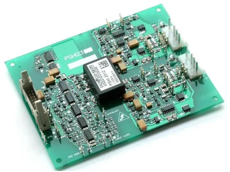
The Art of HDI PCB Design
The art of HDI PCB design is a product of the technological development of the modern electronics industry. The relentless drive for miniaturization and enhanced performance in modern electronics, from smartphones to advanced medical devices, has made High-Density Interconnect (HDI) Printed Circuit Board (PCB) design a critical discipline. Moving beyond the capabilities of traditional PCBs, HDI technology enables the creation of more compact, reliable. And faster boards by incorporating finer lines, microvias, and higher connection pad density.
What Is The Core of HDI Design?
The core of HDI design lies in its sophisticated via structures. Unlike traditional through-hole vias that span the entire board thickness. HDI utilizes microvias—laser-drilled holes with diameters typically less than 150 microns. These are deployed in various stacked or staggered configurations to create intricate routing paths between multiple layers. This approach is fundamental for escaping from fine-pitch Ball Grid Array (BGA) components. Because it allows connections to fan out efficiently without a massive increase in board size. Effective HDI design strategically employs a build-up process, adding sequential layers of dielectric and copper. Which we interconnect them by these microvias. This methodology drastically reduces the need for complex through-hole vias that consume valuable real estate.
What Is A Successful HDI Design?
Successful HDI design is a collaborative effort that requires close integration between the design engineer and the manufacturer from the very beginning. Key considerations include material selection, as high-performance laminates are often necessary for reliable microvia formation and signal integrity. We must established strict design rules for trace width and spacing, annular ring size, and via capture pad dimensions. Furthermore, aspects like signal integrity, power integrity, and thermal management become even more pronounced in such densely packed environments. We must calculate and maintain meticulously the impedance control for high-speed signals across the entire board.
In conclusion, HDI PCB design is no longer a niche skill but a fundamental requirement for developing next-generation electronic products. It represents a paradigm shift from simple connectivity to a holistic, miniaturized system integration approach. By mastering the principles of microvia utilization, sequential build-up. And rigorous design-for-manufacturing, engineers can unlock new levels of performance and functionality, pushing the boundaries of what is possible in the electronic world.