PCBA Stencil
What’s PCB Assembly Stencil?
PCBA Stencils are essential for assembling surface-mount devices (SMDs) onto printed circuit boards (PCBs). To solder components in place, solder paste must be applied to their designated footprints. This is achieved using SMD stencils.
An SMD stencil, also called a PCB stencil, is a thin sheet of stainless steel placed over the board, with openings cut out at the locations of the SMDs. Solder paste is spread across the stencil and transfers through these openings onto the component pads below.
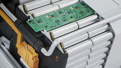
Solder paste printing is a critical step in SMD assembly, as it deposits paste onto the bare board before components are placed.
Lasers are typically used to cut the openings in stencils at the precise positions of the surface-mount components. Solder paste is then applied through these apertures. Previously, wire mesh screens were used, but they restricted aperture size, stencil durability, and printing speed. The adoption of stencils has effectively addressed these limitations.
How about the PCBA Stencil process
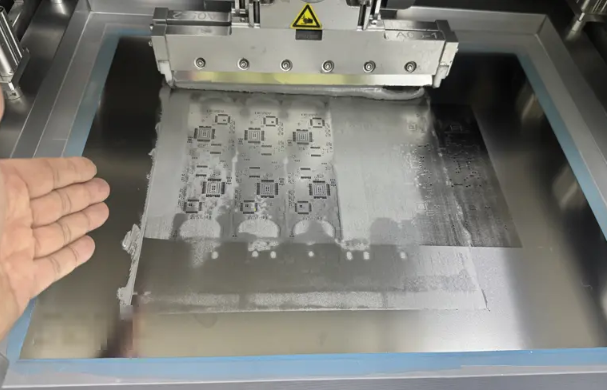
The stencil process begins by aligning the stencil with the PCB using an automated printer. An internal vision system ensures accurate alignment by referencing global fiducials.
Once aligned, solder paste is applied through the stencil openings with a metal squeegee. After removing the stencil, the paste remains deposited on the board, ready for the placement of all SMD components.
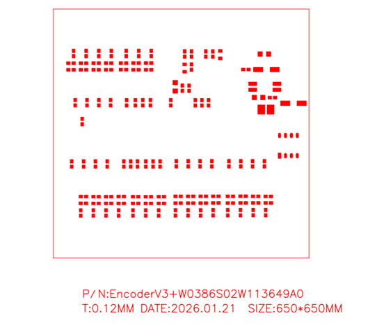
What’s the standard thickness for a solder paste PCBA stencil?
A solder stencil is typically 0.006 to 0.010 inches thick, which matches the intended height of the solder paste deposit.
If the stencil is too thick, solder paste may not transfer properly to the board, as surface tension can cause paste to stick inside the apertures. These factors should be considered when determining stencil thickness.
- A stencil’s effectiveness is measured by its transfer efficiency.
- How effectively does solder paste transfer to the circuit board through the stencil openings?
- This is the primary consideration in both stencil design and selection.
- In an ideal scenario, all solder paste applied to the aperture should transfer fully to the PCB surface.
- However, in practice, the deposited solder paste volume often deviates from the expected volume.
- This relationship is defined as transfer efficiency, expressed by the following formula:
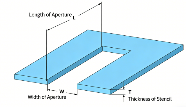
Transfer efficiency=Actual printed volume/Theoretical maximum volume
- The theoretical maximum volume equals the volume of the stencil aperture.
- Ideally, transfer efficiency should equal 1.
- In real applications, however, the value is typically less than 1.
- The goal is to make this value as close to 1 as possible to achieve optimal transfer performance.
What are SMT Stencils Made of?
SMT stencils are typically fabricated from stainless steel, although nickel may occasionally be used depending on the manufacturing process. The selection of material and method is often based on specific application requirements, with the most widely adopted approach described below.
Laser-Cut PCBA Stencils
Laser-cut stencils are SMT stencils whose apertures are precisely formed using laser technology. They are commonly produced from stainless steel. This method offers several advantages, including high precision, fast processing times, and excellent dimensional accuracy in aperture creation.
Advantages of Laser-Cut PCBA Stencils
The inner walls of laser-cut apertures are often finished with electro-polishing or nickel plating to enhance surface quality and solder paste release. Unlike some alternative methods, laser cutting eliminates the need for photomasks, thereby simplifying the production process. Additionally, this technique ensures high consistency in aperture geometry, resulting in greater reliability.
A notable feature of laser-cut apertures is their trapezoidal cross-section, which is widely recognized for promoting efficient and uniform paste release.
Electroformed (E-FAB) PCBA Stencils
Another manufacturing method is electroforming (E-FAB), a nickel-based process used to produce stencils with smooth, gradually tapered aperture walls. This technique also forms a slight ridge along the bottom edge of the aperture, which can help improve solder paste transfer efficiency.
Stencil Maintenance and Storage for PCBA Stencil
After each use, stencils should be thoroughly cleaned to remove any residual solder paste. They must then be stored in a controlled environment to prevent contamination or damage, and carefully inspected prior to reuse to ensure print quality and consistency.
Contact Suga for Stencil quote!