What is the Electroplated Nickel Gold for PCB?
Electroplated Nickel Gold for PCB is a surface finishing technology where a layer of nickel is first electroplated on the PCB copper foil, followed by a layer of gold on the nickel layer. Its core roles are to protect the copper surface, enhance electrical conductivity, and improve soldering/contact reliability.
Core Principles and Process Steps
Electroplated nickel gold is not accomplished in a single step. Instead, it achieves functional complementarity through a dual-layer structure of “nickel base layer + gold coating”. The typical process flow is as follows:
- Pre-treatment: The PCB copper surface is cleaned and micro-etched to remove oxide layers and impurities, ensuring the adhesion of subsequent coatings.
- Electroplating Nickel: The PCB is placed in a nickel salt solution, and a nickel layer (typically 2–5 μm in thickness) is deposited on the copper surface via electrolysis. The nickel layer mainly functions to isolate copper from gold, preventing copper diffusion into the gold layer (which would impair performance), while also enhancing the wear resistance of the overall coating.
- Electroplating Gold: Electrolysis continues on the nickel layer surface to deposit a gold layer (typically 0.05–0.5 μm in thickness). The gold layer boasts excellent electrical conductivity, oxidation resistance, and chemical stability, enabling it to maintain good soldering or contact performance over an extended period.
- Post-treatment: Steps such as cleaning and drying are performed to remove residual chemical solutions and ensure coating quality.
Core Characteristics and Application Scenarios
The advantages of electroplated nickel gold align well with its application scenarios, mainly reflected in the following aspects:
- High Reliability: The gold layer has strong oxidation resistance. Even during long-term storage or in harsh environments, it can maintain stable electrical connections. It is suitable for components requiring long-term reliable contact, such as high-frequency connectors and key contacts.
- Excellent Solderability: Gold bonds well with solder, reducing issues like cold solder joints and pseudo solder joints. It is often used in high-precision soldering areas such as BGA (Ball Grid Array) and IC pins.
- Strong Wear Resistance: The nickel layer has relatively high hardness. Combined with the low friction coefficient of the gold layer, it can withstand repeated insertion/extraction or contact friction. It is suitable for easily worn positions such as slots and probe test points.
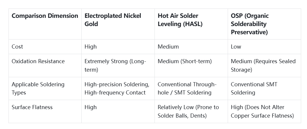
However, it also has obvious limitations: Its cost is much higher than that of surface finishing processes like Hot Air Solder Leveling (HASL) and Organic Solderability Preservative (OSP). Moreover, an excessively thick gold layer may cause the “gold embrittlement” issue, which affects solder joint strength.
The Main Differences Between Electroplated Nickel Gold for PCB and Other Surface Treatments