
Step into the precise world of high multi-layer PCBA
The Definition and Importance of High Multi-layer PCBA
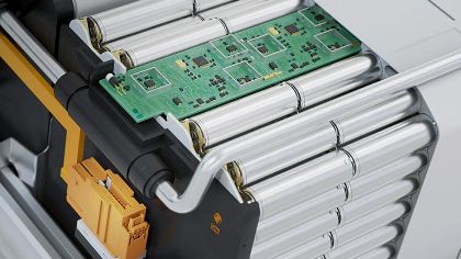
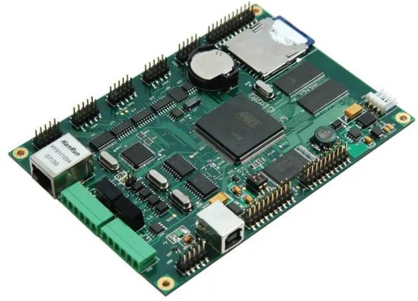
High multi-layer PCBA is an indispensable core engine for modern high-end electronic devices. From smart phones to artificial intelligence servers, these powerful yet compact devices all rely on this highly integrated precision circuit board inside. When traditional double-sided or four-layer boards fail to meet the complex wiring requirements, high multi-layer PCBA emerges.
Figurative metaphor of High Multi-layer PCBA
We can compare this kind of precision circuit board to a modern “high-rise building complex”.Ordinary circuit boards are like low bungalows, with limited space for wiring. High multi-layer PCBA, on the other hand, is like a series of skyscrapers. It interconnects up to dozens of layers of precise copper wires. This builds a complex circuit network within a limited area, forming the “city skyline” inside electronic products.
Technical advantages and application fields
This three-dimensional structural design brings significant advantages: performance breakthroughs, providing stable and high-speed signal transmission channels for core chips such as cpus and Gpus; Spatial optimization has greatly increased the density of circuit layout, making terminal devices increasingly thin and light. The designers enhanced the anti-interference function. The dedicated power layer and ground layer effectively shield electromagnetic noise, ensuring the long-term stable operation of the equipment.
It is precisely because of these advantages that high multi-layer PCBA has become an important cornerstone in cutting-edge fields such as 5G communication, artificial intelligence, high-end computing and medical devices. Its design and manufacturing level is an important indicator to measure the technological strength of the electronics industry, driving the innovative development of the entire intelligent era.
Professional manufacturing partner -Suga
To scale the heights of science and technology, reliable partners are needed. Suga has been deeply engaged in the manufacturing of high multi-layer PCBA. With advanced process technology and strict quality control, it builds stable and reliable “precision high-rise buildings” for you.
Join hands with Suga and give your innovative products a head start. With exquisite craftsmanship and considerate service, we help our clients stand out in the fierce market competition.