
How to reduce the cost of PCBs?
Although it may seem simple, designing a fully functional and commercially viable printed circuit board requires a detailed understanding of various factors that affect the cost of the PCB. Designers may be able to freely add all the high-spec components they desire, but their design will be constrained by the cost of the PCB board, and this is for good reasons. To maximize profit margins, the cost of the product must be reduced. In most cases, the PCB is an important component of the product cost. Therefore, the cost of the PCB must be reduced as much as possible. This article will briefly discuss the techniques adopted by designers and organizations to minimize the price of the PCB.
Impact of Design and Procurement on the PCB cost
The final cost of the printed circuit board depends on the actions and decisions made by the designers and the purchasing team.
The factors that designers influence in the cost of PCB boards include the following aspects:
- Layer stack
- Material
- Size
- Surface treatment
- PCB shape
- Types of components on the PCB
- Features like ENEPIG, IC substrate, etc
The factors that the procurement team influences regarding the cost of PCB boards include the following aspects:
- Order volume
- Shipping location and manufacturer location
Measures to reduce the PCB cost
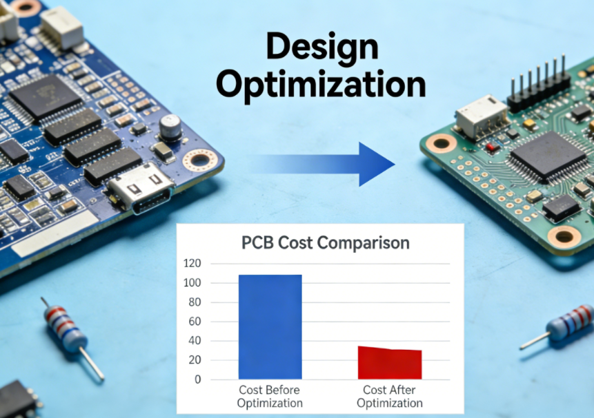
There are several ways to reduce or optimize the cost of PCBs. Through various methods, the cost per square inch of the PCB can be lowered, making the cost for the designers lower and achieving the desired final product. As mentioned earlier, some measures need to be handled by the designers, while others need to be handled by the purchasing team.
The designer can achieve PCB cost reduction by:
Mindful Use of Features:
Designers must use Features mindfully and moderately to reduce the cost of printed circuit boards. Using features such as blind holes and buried holes will increase the manufacturing cost of the circuit board. It should be understood that most circuit boards do not require high-end functions, but this does not mean that these functions cannot be used when necessary.
Only minimize the size when it is truly necessary:
Although smaller-sized PCBs have lower costs, reducing the size of the pcb does not always lead to a lower quote. The principle is that when the line width, via hole size, and pin spacing are below a certain threshold, costs will increase, which could even offset the potential savings that might have been achieved on a smaller-sized circuit board.
Optimal Utilization of Layer Stack:
Most ordinary PCBs usually remain on double sides, while high-speed PCBs are best kept at a maximum of 4 layers. There are reasons for designers to limit the use of layers. Unnecessary increase in the number of layers will also raise the cost and complexity of the PCB. Of course, designers should not hesitate to use more layers when they consider it absolutely necessary. Additionally, it is recommended that designers not use peculiar or uncommon layer stacks, as they may be more costly than common layer stacks.
Best way to utilize copper:
Increasing the thickness of copper in any layer will increase the manufacturing cost of the PCB. It is advisable to use wider traces and copper layers pouring instead of using thicker copper in the PCB to enhance the current-carrying capacity of the traces.
Use appropriate surface treatment to reduce PCB cost:
The surface treatment process is an important component of the cost of PCBs. Designers must determine the surface treatment method required for their designs. Surface treatment processes like ENEPIG can provide very reliable outputs, however, such processing methods are costly and may not be necessary for most designs. Common designs with components of wider spacing can use lead-free HASL, while designs with narrower spacing can use ENIG. When using ENIG and ENEPIG, the thickness of gold used in the surface treatment also has an impact on the cost of the PCB board. Increasing the gold density in the surface treatment will increase the cost of the printed circuit board, as well as the durability of the pads and interconnections.
Utilize materials rationally to reduce PCB costs:
Designers should only use rare and high-end materials when absolutely necessary. Even when using FR-4 material, choosing a higher-grade FR-4 will increase the cost of the PCB. For PCBs that require the use of high-end materials (those with similar manufacturing processes to FR-4), designers can also choose a hybrid PCB, where the inner layer uses FR-4 as an isolation layer, and the signal layer uses high-end materials for isolation.
Buyers can reduce PCB cost in the following ways:
Reduce PCB costs through bulk ordering:
The ordering of PCBs follows a simple rule: To reduce the cost of each PCB, the quantity ordered must be larger. It should be noted that sample quantities like 1 to 10 would be very expensive. Bulk ordering can also distribute many management costs among the various PCBs, and multiple bulk orders from one supplier may result in discounts for future orders.
Selecting the manufacturer and its location:
The details of the PCB procurement process are quite complex. As is well known, in some regions, it is extremely difficult for local manufacturers to match Chinese manufacturers in terms of cost and quality, because very complex printed circuit boards simply cannot be manufactured locally. However, many countries impose import tariffs based on the application of electronic products, the nature of the printed circuit boards, and the proportion of assembly performed on the printed circuit boards. India and Europe are good examples. India imposes very high import tariffs on bare printed circuit boards with less than six layers from all over the world, while the member states of the European Union have very low or even no tariffs on imported printed circuit boards; therefore, the same type of printed circuit board from the same source may have different prices in two different places, even without considering transportation costs.
Obtain services from manufacturers:
Including services such as assembly and turnkey sourcing in the consideration scope may enable suppliers to offer discounts for PCB manufacturing. However, apart from the obvious benefits, there are also cost advantages that may reduce the cost per square inch of the PCB. Unassembled bare PCBs are regarded as SKD products or semi-disassembled products, and their tariffs may be lower than that of the bare PCB itself. Adding assembly services not only helps to lower tariffs but also helps to assemble difficult components such as BGA components, otherwise the cost of assembling these components locally would be extremely high.
Summary
There are various methods for controlling PCB costs. In practice, cost reduction actions need to be implemented at all stages of the product’s entire life cycle. To achieve the desired cost optimization effect, in addition to controlling the production and manufacturing process, other supporting measures also need to be taken into account. Here is a professional suggestion for designers: Do not expect to significantly reduce manufacturing costs by making minor changes to the PCB; especially in the case of bulk purchases, the cost reduction effect of each individual board will directly offset the meager benefits brought by these minor changes.