
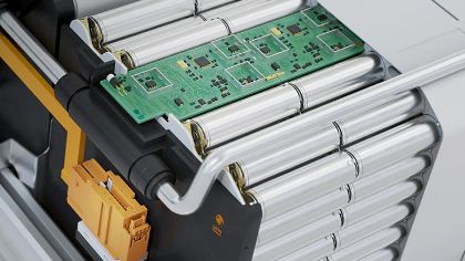
High-frequency and high-speed PCB board
High-frequency and high-speed PCB board:Modern electronic devices “Neural Highway”
In the cutting-edge technology field of 5G,Artificial intelligence,High-speed data center ect,the requirment of Signal transmission speed and frequenc for electronic equipment are constantly rising. The core carrier that carries these key signals–High-frequency and high-speed PCB board,It has become the cornerstone and challenge of modern electronic design
First.What is “High-frequency and high-speed PCB board”
High-frequency:Certainly,High-frequency is the working frequency reached hundreds of MHz to over GHz,The signal wavelength is extremely short
High-Speed:high speed is the extremely steep edge of a digital signal,even the signal frequency not high,its high-frequency components are also extremely rich
Second.Core challenges in design
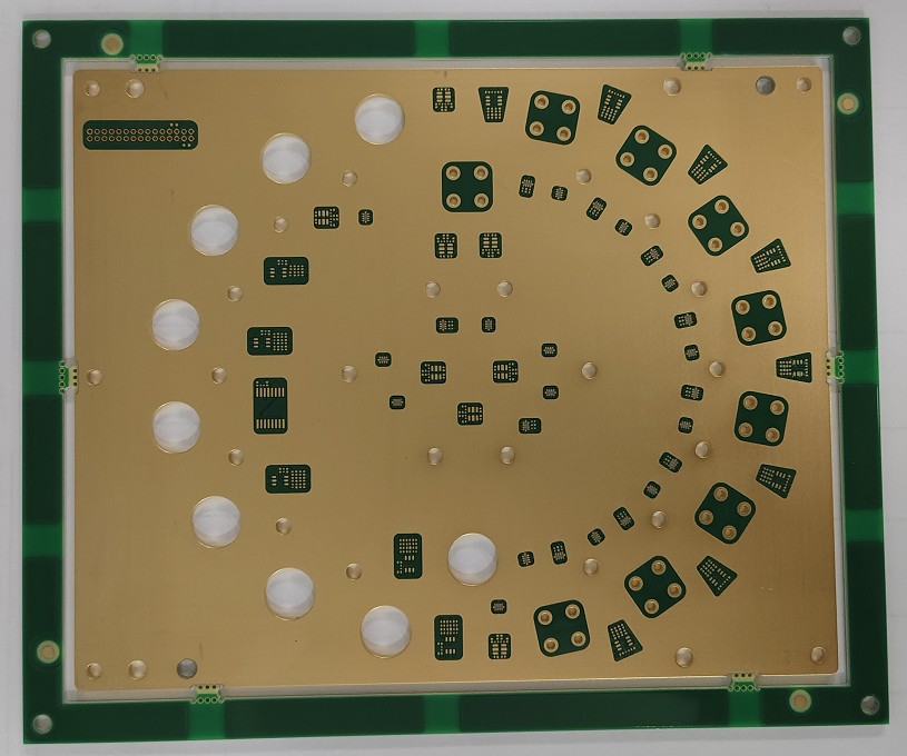
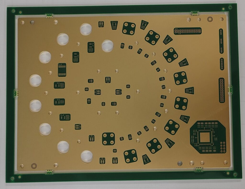
Transmission loss: conductor loss,dielectric loss rising with frequency. low loss materials(such as Rogers,Isola High frequency material). And pricision impedance are very important
Reflection and Distortion: impedance changing will lead to the signal reflect,break the waveform. Strict matched impedance and optimized layout is the core
Crosstalk: In dense wiring, adjacent signal lines interfere with each other. Through increase the space,ground wire shielding and differential wiring are used to suppress
Radiation control:high-speed is a potential noise source.good grounding.shielding and minimizing the loop area are the core strategies for suppressing radiation
3.The key design considerations
Material choose:Low DK can make sure the speed of the signal,Low DF can reduce heat generation and attenuation
Precision manufacture:Undoubtedly,strict tolerance of line width and space,accurated interlevel alignment,Smooth copper foil surface
Via optimize:use backdril,blind buried holes to reduce the Stub effect,optimize the via structure can reduce impedance discontinuity also
Simulation-driven:Rely on professional SI/PI/EMC simulation tools (such as HFSS, ADS, SIwave) to predict and solve problems in the early stage of design
Third.Future trend
As data rates move towards 112Gbps and 224Gbps,and the popularization of millimeter-wave applications,more stringent requirements have been put forward for sheet material loss, Especially manufacturing accuracy, design complexity and 3D electromagnetic simulation.
New materials(such as PTFE,LCP),SIP and automated design tools will become the key to breaking through the bottleneck
Conclusion:
High-speed and High frequency PCB design is a deeply interdisciplinary field of electronic engineering materials science and precision manufacturing.It is the inevitable path to building the next generation of high-performance and highly reliable electronic systems to master its core principles and overcome the design challenges.
Above all: it is the true “invisible highway” that drives the digital world to keep surging forward.