
Heavy Copper PCB Design & Manufacturing: Suga Offers One-Stop Solution
Heavy copper PCB design is a critical enabler for driving performance breakthroughs in high-power electronic devices, as it delivers exceptional current-carrying capacity and efficient heat dissipation. Its manufacturing quality directly impacts the end products’ reliability, safety, and service life—making professional design and precision production essential for high-reliability applications.
1.What is Heavy Copper PCB?
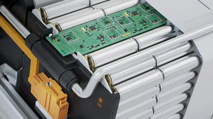
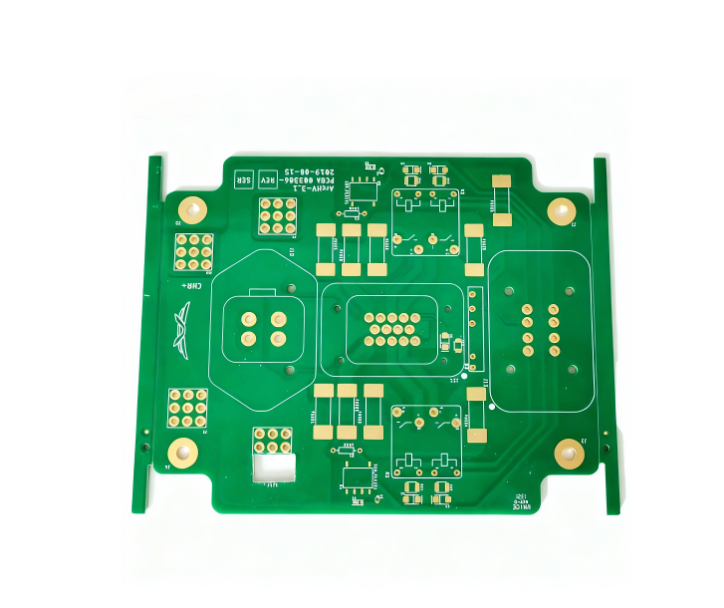
Heavy Copper PCBs refer to printed circuit boards with a copper layer thickness of 3 oz (105μm) or more. Widely used in high-power, high-current applications such as industrial power supplies, automotive electronics, and renewable energy equipment, they differ from standard PCBs notably in their thicker copper layers—even up to 20 oz in extreme cases. These layers offer exceptional current-carrying capacity, efficient heat dissipation, and enhanced mechanical durability, making them core components for high-reliability projects.
2.Key Considerations in Heavy Copper PCB Design & Manufacturing:
Design Aspects
Heavy copper PCB design requires precise optimization of line width and spacing to accommodate thick copper layers. Additionally, thermal management solutions such as thermal vias and copper pads must be integrated to prevent overheating. Furthermore, designers need to consider material compatibility, selecting high-temperature-resistant substrates that match the thermal expansion coefficient of thick copper to ensure long-term stability.
Manufacturing Process
The manufacturing flow includes critical steps:
- Substrate selection
- Copper layer thickening (electroplating or copper foil lamination)
- Precision etching (to ensure circuit accuracy)
- Drilling (specialized tools for thick materials)
- Surface finishing (e.g., electroless nickel gold/ENIG, organic solderability preservative/OSP) to enhance corrosion resistance.
3.Advantages of Suga’s One-Stop Heavy Copper PCB Services
Suga offers end-to-end services for heavy copper PCBs, covering design optimization, prototyping, and mass production. Our professional engineering team provides design reviews to address line width, thermal management, and manufacturability issues. Leveraging advanced equipment, we ensure consistent quality. From initial design to final delivery, we streamline processes, shorten lead times, and implement flexible pricing strategies to mitigate copper price volatility—comprehensively meeting customer needs for high-power projects.