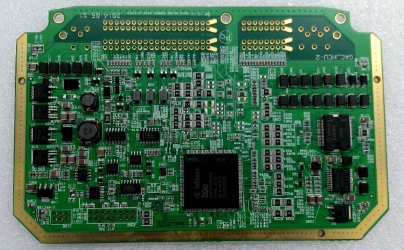
Future Trends in the PCB Industry
Future Trends in the PCB Industry is becoming a hotter topic now. Because the Printed Circuit Board (PCB) industry, a cornerstone of modern electronics, is undergoing a significant transformation driven by technological advancements and evolving market demands. Several key trends are shaping its future trajectory:
1. Miniaturization and High Density
The relentless push for smaller, more powerful, and portable electronic devices is a primary driver. This fuels the adoption of:
1) High-Density Interconnect (HDI) PCBs. Featuring finer lines, microvias, and higher connection pad density, HDI technology is essential for smartphones, wearables, and advanced medical devices.
2) Substrate-like PCBs (SLP). Blurring the line between traditional PCBs and IC substrates, SLPs offer even higher density, approaching the feature sizes of semiconductor packaging.
2. Advanced Materials
The limitations of standard FR-4 materials are becoming apparent for high-frequency and high-power applications. The future lies in:
1) High-Frequency/Low-Loss Materials. Materials like PTFE (Teflon) and hydrocarbon ceramics are critical for 5G/6G infrastructure, automotive radar, and millimeter-wave applications.
2) Thermal Management Materials. Metal-core PCBs (MCPCBs), insulated metal substrates (IMS), and materials with high thermal conductivity are vital for dissipating heat from high-power LEDs, power electronics, and electric vehicle components.
3) Flexible and Stretchable Materials. The use of polyimide (PI) and Polyethylene Terephthalate (PET) will continue to grow. Emerging stretchable substrates will enable new applications in wearable electronics and biomedical implants.
3. Integration and Embedded Components
To save space and enhance performance, the industry is moving towards greater integration:
1) Embedded Components. Passive components (resistors, capacitors, inductors) and even some active chips are being buried within the PCB layers, freeing up surface space and improving electrical performance by reducing parasitic effects.
2) System-in-Package (SiP) and Integrated Circuit (IC) Substrates. The line between PCBs and semiconductor packaging continues to blur. Advanced PCBs are increasingly acting as sophisticated platforms for integrating multiple chips into a single package.
4. Additive and Semi-Additive Manufacturing
Traditional subtractive methods (etching away copper) are facing challenges with ultra-fine features. Additive techniques are gaining ground:
1) Printed Electronics. Using conductive inks to “print” circuits onto flexible substrates enables low-cost, large-area electronics for IoT sensors and smart packaging.
2) Semi-Additive Processes (SAP) and Modified SAP (mSAP). These processes are essential for manufacturing the ultra-fine traces required for HDI and SLP boards, offering superior precision and reduced copper waste.
5. Sustainability and Green Manufacturing
Environmental responsibility is becoming a competitive imperative.
1) Lead-Free and Halogen-Free Materials. Regulations and consumer demand are driving the adoption of environmentally friendly materials.
2) Recycling and Waste Reduction. There is a growing focus on recycling process water, recovering precious metals from waste streams, and designing for disassembly and recyclability.
3) Energy-Efficient Production. Manufacturers are investing in equipment and processes that reduce energy consumption.
6. Automation and Industry 4.0
To achieve higher quality, yield, and efficiency, PCB factories are becoming smarter.
1) AI and Machine Learning. Used for predictive maintenance, defect detection (Automated Optical Inspection), and process optimization.
2) Industrial Internet of Things (IIoT). Sensors throughout the production line provide real-time data for monitoring and controlling the manufacturing process.
3) Full Traceability. Blockchain and other digital systems are being explored to provide complete traceability of materials and processes, which is crucial for automotive and medical applications.
7. Application-Driven Growth
Demand from key sectors will dictate the pace of innovation:
1) Automotive. The transition to Electric Vehicles (EVs), Advanced Driver-Assistance Systems (ADAS), and in-vehicle infotainment requires robust, high-reliability PCBs capable of handling high power and high frequencies.
2) Telecommunications. The global rollout of 5G and future 6G networks demands massive amounts of high-frequency PCBs for base stations and network infrastructure.
3) Internet of Things (IoT) & Wearables. The proliferation of connected devices requires a vast range of PCBs, from simple, low-cost boards to complex, miniaturized, and flexible ones.
4) Medical Electronics. Advanced diagnostic, monitoring, and treatment devices rely on high-density, high-reliability PCBs, with growing demand for flexible and biocompatible options.
The future of the PCB industry is dynamic and innovation-driven. Success will hinge on mastering advanced technologies like HDI, adopting new materials, integrating smarter manufacturing processes, and adapting to the stringent requirements of next-generation applications like AI, 5G/6G, and electric vehicles. The humble PCB is evolving from a simple interconnection platform into a sophisticated, high-value engineered component that is critical to the progress of the entire electronics ecosystem.