
Consumer Electronics PCB Assembly Technology
What is Electronics PCB Assembly?
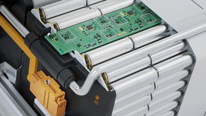
Electronics PCB Assembly (PCBA) refers to the process of mounting electronic components onto printed circuit boards to form functional modules. Its core technologies include Surface Mount Technology (SMT) for micro-components and Through-Hole Technology (DIP) for larger parts. The typical workflow covers four key steps: solder paste printing, automated component placement, reflow soldering, and quality inspection via AOI (Automatic Optical Inspection) or X-ray . This process transforms blank PCBs into the “brains” of consumer electronics.
Shenzhen’s Technical Advantages in Consumer Electronics PCB
As a global electronics hub, Shenzhen leads in PCBA with advanced infrastructure. Local enterprises deploy high-speed placement machines (up to 300,000 points/hour) and 3D SPI detectors, achieving ±0.03mm placement precision . Leveraging industrial clusters, Shenzhen integrates PCB manufacturing, component supply, and assembly, supported by digital MES systems that cut lead times by 25% . It specializes in high-density assemblies for smartphones and wearables, handling 01005 ultra-mini components reliably .
Global Development Trends of the Industry
Globally, PCBA is driven by AI and miniaturization. High-density interconnect (HDI) and 18-layer+ PCBs see 18.8% and 40.2% annual growth , catering to AI servers and 5G devices. Flexible PCBs are increasingly used in foldable electronics . Prismark predicts the global market will reach $964 billion by 2029, with China’s high-end PCB capacity growing at 21.1% CAGR, as automation and smart testing become industry standards .
Synergy of Local Expertise and Global Trends
The evolution of consumer electronics PCBA highlights Shenzhen’s role as both a technological testbed and global manufacturing hub. As HDI, flexible PCBs, and AI-driven automation reshape the industry, thus the future lies in balancing micro-assembly precision with sustainable innovation. Specifically, this requires leveraging Shenzhen’s industrial ecosystem to tackle 3D packaging challenges and green standards, while aligning with global shifts toward intelligent manufacturing. Additionally, emerging applications like IoT edge devices and medical wearables are further pushing PCBA toward ultra-miniaturized, low-power assemblies, driving demand for advanced heterogeneous integration technologies. Moreover, PCBA has evolved from a process to a critical bridge between component innovation and next-gen devices. Ultimately, its evolution underscores the need to integrate technological rigor with sustainable practices in the global manufacturing landscape.