
Surface Mount Technology in China
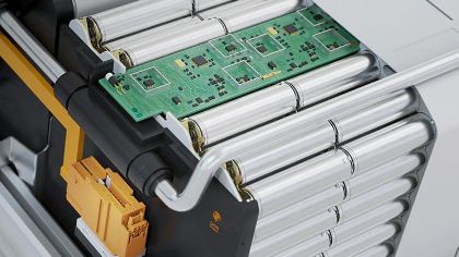
Surface Mount Technology in China, is the essential process of transforming a bare PCB into a functional electronic brain. It’s the crucial bridge between design and a working product. While a PCB provides the pathways for electrical signals, it is the components attached to it that bring it to life. The assembly process is a precise and automated sequence, primarily involving SMT (Surface Mount Technology) and THT (Through-Hole Technology). Understanding PCBA is fundamental for anyone involved in electronics creation, from engineers to project managers, as it directly impacts product quality, reliability, and cost.
The Core Stages: SMT and Beyond
The journey begins with SMT. First, a stencil is used to apply solder paste onto the PCB’s pads. Next, a high-speed pick-and-place machine accurately positions tiny surface-mount components like resistors, capacitors, and integrated circuits onto the paste. The board then travels through a reflow oven, where carefully controlled heat melts the solder, creating permanent electrical connections. For larger components requiring mechanical strength, such as connectors, a secondary process called THT is used. These components are inserted into holes and soldered, often using a wave soldering technique.
Why DFM is Non-Negotiable Surface Mount Technology in China
A perfect design on software can fail in production without Design for Manufacturability (DFM). DFM is the practice of designing the PCB layout to optimize the assembly process. Key considerations include component spacing to avoid soldering issues, appropriate pad sizes to prevent defects like “tombstoning,” and panelization for efficient manufacturing. Ignoring DFM leads to low yields, higher costs, and delayed time-to-market. Early collaboration between design and manufacturing engineers is vital to identify and resolve potential production challenges before they become expensive problems.
Ensuring Reliability: Inspection and Testing
Rigorous inspection and testing are the final, critical steps to ensure quality. Automated Optical Inspection (AOI) uses cameras to check for missing components, misalignment, and solder defects. For complex chips with hidden solder joints, like BGAs, X-ray inspection is necessary. Electrical testing is then performed. In-Circuit Test (ICT) verifies the correct value and placement of individual components, while Functional Circuit Test (FCT) simulates the final operating environment to confirm the board performs as intended. This multi-layered approach is essential for delivering reliable products to the end-user.
In conclusion, PCBA is a sophisticated symphony of technology and precision. Mastering its stages, prioritizing DFM, and implementing thorough testing are the pillars of successful electronic product development.
