What is the difference between HDI boards and ordinary PCB boards?
Today, smartphones are more than 6 mm thick and pacemakers are smaller than a button, and cutting-edge substrates called HDI (high-density interconnect) boards support these electronic wonders. Compared with traditional PCBs (printed circuit boards), HDI technology is reshaping the physical limits of the electronics industry. This difference can be attributed to three dimensions: spatial reconstruction, signal revolution, and manufacturing transformation.
Spatial Density:

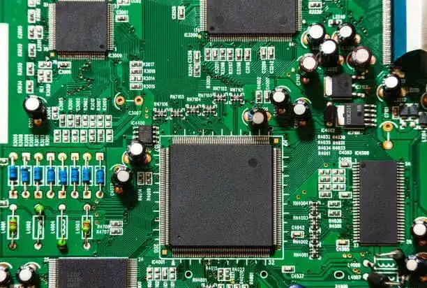
Ordinary PCBs are like multi-story apartment buildings, relying on “stairwells” (mechanical drilling) that penetrate the floor slabs to achieve inter-layer interconnection. These holes, which are usually larger than 0.2mm in diameter, not only take up valuable board space, but also force the wires to take detours, resulting in limited wiring density – the line width/spacing is mostly above 100μm.
HDI boards are like precise three-dimensional transportation hubs: laser ablation technology is used to punch out micro-holes as thin as hair (<0.1mm), and a composite structure of blind holes (from the surface to the inner layer) and buried holes (between inner layers) is used. Combined with ultra-fine wiring with copper wire width reduced to less than 75μm, the circuit complexity in the same area has increased by 2-3 times. For example, the motherboard of a flagship mobile phone is only the size of a fingernail, but it can accommodate the interconnection needs of 1 billion transistor chips.
Signal Transmission:

The signal transmission of traditional PCB is like a vehicle going around a multi-layer roundabout. The long-distance via path causes signal delay and attenuation, and is susceptible to electromagnetic interference in high-frequency scenarios, which restricts the breakthrough of 5G/6G communication equipment performance. The HDI board shortens the signal transmission distance by more than 60% through the micro-hole short-distance interconnection architecture, and combines the any-layer stacking technology (Any-layer HDI) to achieve point-to-point direct connection between the layers of the entire board. This “zero detour” topology greatly improves signal integrity and can stably transmit millimeter waves above 40GHz, becoming the core carrier of autonomous driving radar and space satellite payloads.
Manufacturing Paradigm:

Ordinary PCBs rely on mechanical drills for drilling and etching processes, with an error tolerance of ±50μm, and the yield rate drops significantly above 8 layers. Its advantage is that the cost of a single board is low, and it is suitable for low-complexity products such as power adapters.
The HDI production line operates as a nano-scale ‘photon operating room’: ultraviolet lasers ablate micro-channels with microsecond pulses at ±5μm precision, while semi-additive plating technology directly ‘grows’ ultra-fine copper traces onto insulating substrates.Although the initial R&D cost is 30%-50% higher, its system-level integration advantage brings higher cost-effectiveness in space-constrained scenarios such as smart watches and capsule endoscopes.
Summary of core differences:
Physical structure: HDI uses laser microvias to replace mechanical through-holes to achieve three-dimensional high-density wiring
Electrical performance: Microvia short paths ensure high-frequency signal integrity and reduce latency by 40%
Manufacturing process: Ordinary PCBs are suitable for etching/drilling, while HDI relies on laser direct writing and precision electroplating
Evolutionary logic: Functional electronics → ordinary PCB | Smart hardware → HDI board

