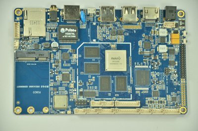
Printed Circuit Board Layout
Printed Circuit Board layout is a critical step in electronic engineering design and is key to enhancing the reliability of electronic designs. Excellent routing can significantly improve circuit performance, reliability, and noise immunity. Proper routing requires not only ensuring accurate electrical connections but also balancing multiple factors such as signal integrity, thermal management, and electromagnetic compatibility. Mastering scientific routing techniques is essential for designing high-performance circuit boards.
Scientific Layout is the Foundation
The component placement prior to routing determines the success of the entire wiring process. A functional modular zoning approach should be adopted, with related components grouped together. We must place high-frequency devices as close as possible to the IC pins to shorten signal paths. Analog and digital circuits should be partitioned and laid out in separate areas to prevent cross-interference. We ought to position the power supply module near board-edge connectors, while high-power components require careful consideration of heat dissipation needs.
Adhering to Layout Specifications is Critical
We should determine the width of signal traces based on their current-carrying capacity. For ordinary signal lines, we typically use a width of 0.2–0.3 mm. Power traces require increased width, with an empirical rule of 1 mm per ampere of current. Avoid 90-degree right-angle bends in traces; instead, use 45-degree miters or arc angles to reduce signal reflection and electromagnetic radiation. We should keep high-frequency signal lines short and straight, and should employe serpentine routing where necessary to achieve length matching.
Grounding System in Design Printed Circuit Board Layout
A robust grounding scheme is critical for ensuring signal integrity. A star grounding topology or ground plane approach is recommended to prevent ground loops. We should route digital and analog grounds separately and connected at a single point using a ferrite bead or zero-ohm resistor. Place 0.1μF decoupling capacitors near the power pins of each integrated circuit, and position a 10–100μF bulk capacitor at the power entry point.
Multilayer PCB Design Strategy
Modern high-density PCBs typically employ a 4 to 6-layer design. The most experienced designers usually recommend to route adjacent signal layers with perpendicular trace orientations to reduce interlayer crosstalk. We should use dedicated power and ground planes to form stable reference planes. When designing, we should keep sensitive signal traces away from noise sources such as clock lines and switching power supplies, and we should apply shielded protection when necessary.
Critical Signal Routing
Differential pair traces should maintain parallel routing, equal length, and consistent spacing, with impedance matching being critical. We should priority clock signals should during routing and keep it away from sensitive circuits. For high-frequency signals, we recommend to use microstrip or stripline structures with tightly controlled characteristic impedance.
Through systematic routing planning and meticulous implementation, we can enhace the signal integrity of the circuit board can be significantly, electromagnetic interference reduced, and product reliability and stability improved. Excellent routing design is not only a technical practice but also an embodiment of engineering art. It requires designers to continuously accumulate experience and perfectly integrate theoretical knowledge with practical application.