
Ensuring Quality: How Flying Probe Testing Works in PCB Assembly
Flying Probe Testing PCBA (FPT) is an electrical verification method applied to printed circuit boards, especially suited for low-volume manufacturing or prototype stages. As a PCB designer, understanding this inspection process facilitates strategic positioning of test access points, thereby promoting faster and more reliable testing outcomes..
Key Points:
- FPT serves as a fixtureless substitute for In-Circuit Test (ICT), making it well-suited for low to medium production runs and prototype PCBA.
- This method can detect various faults such as open circuits, short circuits, resistance, capacitance, polarity errors, micro-shorts, and phase discrepancies.
- Main elements of FPT systems consist of probes, test fixtures, and control software, which handle program development, probe path optimization, and data evaluation.
- FPT provides advantages like improved test coverage, adaptability to design modifications, and cost efficiency for smaller batch sizes.
This article outlines the stages of FPT and offers practical design recommendations for creating test points that support precise electrical verification.
1.Why ICT is Not Suitable for Low-Volume PCB Production
In-circuit testing (ICT) is a white-box testing approach that validates the operation of a completed printed circuit board assembly. It employs electrical probes to detect faults like short circuits, open connections, and deviations in resistance, capacitance, and other fundamental electrical properties.
Conventional ICT typically depends on a “bed of nails” fixture system, which involves creating a dedicated fixture for each PCB design. This fixture includes spring-loaded pogo pins that are carefully positioned to connect with designated test points on the assembled board. Each pogo pin tests an individual node or test point on the PCB.
Developing a custom ICT fixture for a new PCBA design can be expensive and slow, particularly for complex boards, as fixture production may take multiple days. Consequently, ICT is most advantageous for large-scale manufacturing. For low-volume batches or prototype assemblies, it is neither economical nor practical.
To overcome these challenges, manufacturers often adopt the flying probe testing method.
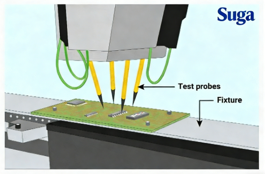
2. What is Flying Probe Testing PCBA?
Flying probe testing (FPT) utilizes movable test probes that travel between predefined test points according to software instructions written specifically for the board being tested.
Since no custom fixture is needed, FPT can also be described as a fixtureless in-circuit test when applied to assembled PCBs. This makes it a highly cost-effective solution for prototypes and low- to medium-volume production.

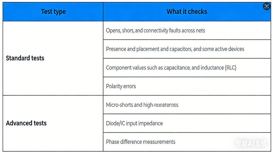
The table provided outlines the inspection capabilities of Flying Probe Testing.
Table 1: Comparison of standard and advanced flying probe test types
Most flying probe testers include integrated cameras to enable automated component polarity verification.
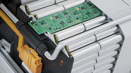
At Suga, our flying probe testing utilizes the Seica S.p.A. Pilot V8 system. This sophisticated equipment offers superior performance, increased testing speed, and is well-suited for low- to mid-volume production. Its capability for vertical probing on both sides of the PCB simultaneously speeds up debugging and enhances flexibility in prototyping.
It can process circuit boards up to 600 x 540 mm in size and mount components up to 40 mm high on both sides. ODB++ files are required for flying probe testing.
To learn more about flying probe testing in PCB assembly, visit the relevant page for further information.
2.1 Components of Flying Probe Testing PCBA Test Systems
A flying probe tester achieves rapid and precise printed circuit board inspection through the coordinated operation of three core components.
- Probes: These serve as the contact points between the tester and the circuit board. Probes transmit signals for measurement and analysis, and can move along the X, Y, and Z axes to reach pads and vias. Common types include:
- Spring Probes (Pogo Pins): Cost-effective and reliable, suitable for standard testing.
- Active Probes: Equipped with internal electronics for high-frequency or highly sensitive measurements.
- Kelvin Probes: Four-wire probes designed for precise low-resistance testing.
- Test Fixtures: Fixtures securely hold the PCB in place during testing to ensure accurate probe contact and prevent false readings or damage. Common types include:
- Mechanical (Universal) Fixtures: The most widely used type, constructed with a rigid frame, clamps, and support pins. They are straightforward and economical but require manual adjustment.
- Control Software: This software coordinates probe movement, fixture control, and data processing. Its key functions are:
- Generating test programs from formats such as ODB and IPC-2581.
- Optimizing probe paths to increase testing speed.
- Performing data analysis and generating reports, including pass/fail results and SPC charts.
- Integrating with systems like AOI, X-ray inspection, or pick-and-place machines.
- Providing a user interface and debugging tools for real-time monitoring, error logging, and test optimization.
2.2 Six Advantages of Flying Probe Testing PCBA
- Cost-effective for small batches: Flying probe testing offers greater economic efficiency compared to In-Circuit Test (ICT) for prototyping and limited production quantities.
- Superior accessibility: Flying probes can contact much smaller pads and component leads than ICT pogo pins, eliminating the need for dedicated test points.
- Adaptable testing approaches: Since probe movement is governed by software, test programs can be easily updated or probe contact positions adjusted without modifying hardware.
- Enhanced test coverage: By directly accessing component pins, flying probes achieve wider test coverage than ICT methods.
- Non-destructive method: The gentle contact of the probes significantly reduces the potential for damaging delicate PCBs or sensitive components.
- Scalable and forward-compatible: Systems can be expanded with additional probes or enhanced software capabilities to accommodate increased production volumes and more intricate designs.
3.ICT versus Flying Probe Testing (FPT)
Table 2: A comparison between In-Circuit Testing (ICT) and Flying Probe Testing (FPT) within the context of PCB assembly
4.The Process of Flying Probe Testing PCBA
The following steps outline the procedure your assembly facility implements to examine a printed circuit board using the Flying Probe Test (FPT) method:
Step 1: Test Program Development
Every FPT system operates with a test program generation application that functions on a personal computer.
This process requires two essential inputs:
- A Bill of Materials (BOM) provided in Excel format.
- Intelligent CAD production files, such as ODB++ or IPC-2581.
After the test program is successfully created, it is uploaded into the tester. The assembled circuit board (whether an individual unit or a panel of multiple boards) is then positioned on a conveyor system, which transports it into the tester’s inspection zone where the probes are situated.
Step 2: Executing the Test
Once the test program is initiated, the probes—directed by the software—establish contact with:
- Pads on components
- Dedicated test pads (where present)
- Exposed vias
Subsequently, the tester delivers electrical test signals and power to these contact points and records the resulting measurements.
Step 3: Analyzing the Results
The tester analyzes the collected measurements to assess whether the tested circuit section functions correctly, in accordance with the installed components and within the defined tolerance limits.
To perform this analysis, FPT equipment integrates several key instruments:
- Signal generators
- DC and AC power sources
- Multiple types of sensors
- Signal multiplexing systems
- Digital multimeters
- Frequency counters
These tools supply stimulus signals to circuit nodes and acquire measurement data from components and their interconnections.
Utilizing a virtual isolation method, the tester applies excitation signals to electrically separate—as much as possible—the circuit segments between the probes from the surrounding circuitry. This enables component values to be measured with high accuracy without the need for physical desoldering.
FPT aims to test the board as thoroughly as the design’s physical layout permits. For foundational design principles, refer to Mastering the Art of PCB Design Basics.
5.Types of Flying Probe Testing PCBA Systems
Flying probe test equipment is available in multiple configurations, each designed to meet particular printed circuit board testing requirements. Selecting a system involves considering various factors, including:
- Complexity of the circuit board
- Production quantity
- Available factory space
- Budget constraints
The following table outlines the primary categories of flying probe test systems, describing their key characteristics, benefits, drawbacks, and typical applications.
Table 3: Comparison of Different Flying Probe Test System Types
6 Key Guidelines for PCB Engineers to Design FPT Test Points
To ensure reliable and accurate Flying Probe Testing, PCB designers must meticulously plan the placement of test points and the overall board layout. The following six guidelines offer practical recommendations to optimize PCBs for FPT.
1. Select Appropriate Test Point Features and Sizes
Choose test points that enable dependable contact with FPT probes.
- Opt for contact locations most compatible with FPT, including:
- Test pads without solder mask covering.
- Vias.
- Through-holes.
- PTH (Plated Through-Hole) and SMD (Surface Mount Device) component pads.
- Define the dimensions and spacing for each test point to guarantee consistent probe contact.
- The minimum recommended size is 6 mils (with 20 mils being preferable). The ideal size also depends on the probe type used. Always consult and adhere to the recommendations provided by your assembly partner.
- The spacing between adjacent test points should be at least 10 to 20 mils.
- Ensure vias are suitable for direct probe contact.
- The via diameter should fall within 8 to 20 mils (with 10 mils being the recommended target).
- Vias must remain clear of solder resist (solder mask).
- For SMD pads smaller than 25 mils, request your manufacturer to extend the solder pad beyond the component pin’s footprint. This allows the probe to contact the pad itself instead of the pin, enhancing test reliability. Clearly specify this requirement in your PCB fabrication notes.
2. Comply with Maximum Board Size Limits
Ensure that the PCB dimensions fall within the specified limits of the testing equipment:
- For the Pilot L4 model: The maximum allowable size is 600 mm by 1010 mm.
- For the Pilot V8 model: The maximum allowable size is 600 mm by 540 mm.
Boards that are larger than these specified limits may not be properly secured within the tester or could obstruct the movement of the probes. It is essential to verify the final board dimensions with your assembly service provider.
3. Incorporate Component Height Data into Your CAD Files
Include the height information for all components within your CAD data to guarantee compatibility with the testing machine.
Consult with your manufacturer to determine the specific model of flying probe tester they utilize. Then, verify that the component heights documented in your CAD data meet the physical clearance requirements of that particular tester model.
4. Maintain Optimal Clearance Between Test Points and Components
Sufficient clearance is essential to avoid probe misalignment or the risk of short circuits. Use the following guideline to calculate the required distance:
The minimum distance (L) between the center of a test point and any nearby component can be estimated with the formula:
L = (0.29 × component height in millimeters) + 0.7 mm
5. Accurately Position Fiducials for Reliable Alignment
To achieve precise probe alignment during the testing process, fiducials must be accurately placed on the PCB. Follow these core recommendations for optimal placement:
- Use two fiducials per board.
- Position these fiducials on opposite sides of the board. Arranging them differently from each other is crucial to effectively eliminate potential side-specific alignment errors.
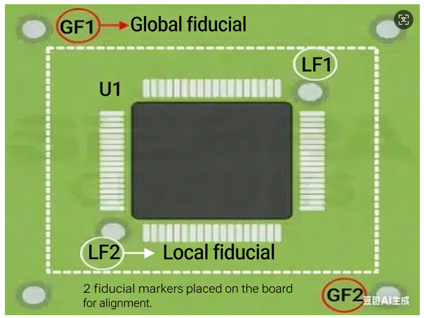
For large boards exceeding 400 mm in dimension, incorporate local fiducials in the vicinity of fine-pitch components. These fiducials must remain visible after the components have been mounted.
6. Prevent Trace Interference with Test Points
Route PCB traces with care to avoid any conflict with designated probe contact locations. Do not run traces in a manner that blocks pads or vias intended for FPT probing. Maintaining adequate clearance around test points ensures uniform test coverage and minimizes the potential for measurement inaccuracies.
To discover methods for preventing assembly delays and additional expenses, please download our comprehensive design guide.
7. Emerging Advanced Features in Flying Probe Testers
1. Phase Difference Measurement Unit
The Phase Difference Measurement Unit (PDM) introduces a high-frequency signal between a reference line and a segment of the signal line. It subsequently measures the resulting phase shift of the signal at the far end to determine the phase difference. This approach can decrease the requirement for traditional isolation testing within a single net.
2. High Voltage Stress Flying Probe Testing PCBA
The High Voltage Stress Test (HVS) is engineered to identify high-resistance isolation faults that might escape detection by the PDM. HVS functions by applying high-voltage pulses between signal lines to expose such defects. A key benefit shared by both PDM and HVS is that they examine each net only a single time, enabling rapid test execution.
3. Micro Shorts Detection
During isolation testing, the abrupt application of a high voltage can cause components with micro-shorts to burn out. Micro short tests prevent this type of damage by ramping up the applied voltage gradually from a low initial level.
In certain scenarios, high-resistance shorts concealed between multiple board layers can behave similarly to semiconductor junctions or capacitors. Applying a high voltage and then reversing its polarity can help reveal these hidden defects.
Key Takeaways:
- In-Circuit Test (ICT) utilizes customized bed-of-nails fixtures equipped with pogo pins to examine assembled boards. This makes ICT highly suitable for high-volume manufacturing, though it can be expensive and time-intensive for prototyping.
- Flying Probe Test (FPT) offers a fixture-free alternative. It operates by moving probes between designated test points under software control, providing a highly cost-effective solution for low-to-medium volume production and prototype boards.
- Essential guidelines for PCB designers regarding FPT test points encompass ensuring net accessibility, selecting and sizing test points appropriately, positioning components correctly, planning for board clamping, adhering to maximum board dimensions, maintaining minimum clearances, placing fiducials accurately, and routing traces to avoid interference.
- FPT programs are generated offline using CAD/ECAD files and Bill of Materials (BOM) data. These programs are then executed on the tester, where the probes make contact with designated pads, test points, and vias.
Flying Probe Testing PCBA has emerged as the preferred, economical solution for low-volume and prototype PCB assemblies. Continuous technological progress is expanding test coverage, enhancing quality assurance, and reducing testing duration, solidifying FPT’s role as a powerful tool for shortening product design cycles and accelerating time-to-market.
Need help with your PCB design? Submit your questions on our expert forum, Suga Connect, for detailed assistance.